
Equipment ASETS Equipment
TOOL Line Up; AETS(Advanced Semiconductor Equipment Technology Singapore Pte.Ltd)
Plasma Etcher, MOCVD, HTCVD, LPCVD, Measurement
*Lab facility is fully equipped with system line for Demo and R&D. (www.asets.com.sg)
ICP ETCH
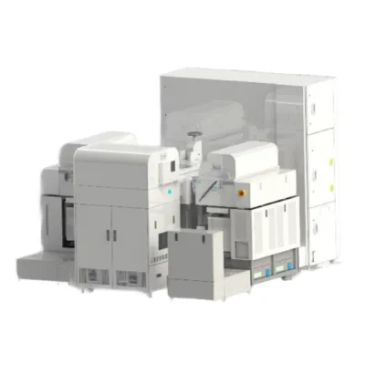
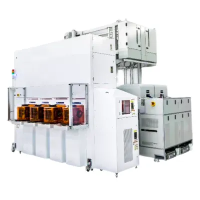
Primo iDEA
Integrated Dual-Station Etch and Asher
Combines D-RIE or AD-RIE process modules with Downstream Asher(DsA) chamber
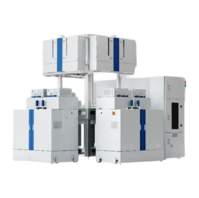
Primo Twinstar
3Dual Station Chamber, High Aspect Ratio(HAR), Surperior control
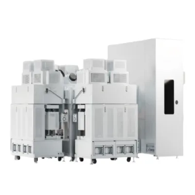
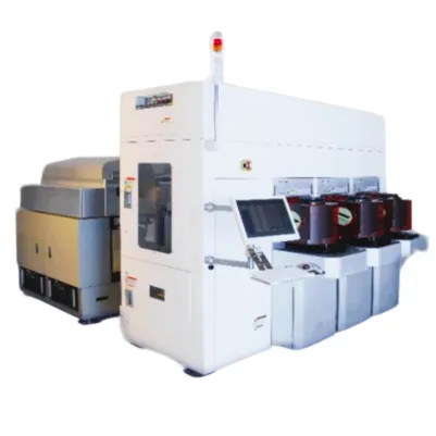
Primo TSV
High density plasma, High productivity for deep silicon etching
For CIS, MEMS, 2.5D, 3D IC
CCP ETCH
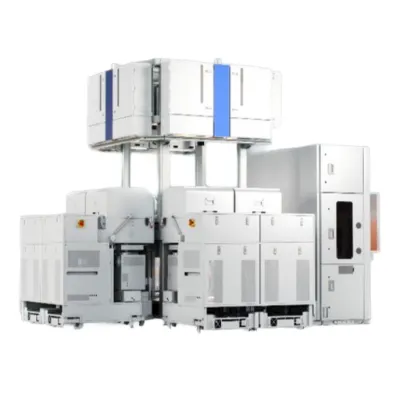
Primo SSC AD-RIE
Mass production on 16nm chip production lines
Primo Primo HD-RIE
High Aspect Ratio(HAR) for 3D NAND, DRAM
Primo D-RIE
45/28/20/15/10nm and below nodes
Inspection, Measurement Particle Labs CVS
Breaking commonsense of particle visualization
Visualizing particles is essential to detect 「Mie Scattering」which can catch unvisible foreign substances. Visualizing for high accuracy requires the ideal installment that light source and camera should be located opposite for maxmization of scattered light streangth.
However, in conventional system, these size of light source and camera become an obstacle, we face the difficulty on ideal setting in limited space facility.
This product can reach to the world smallest, lightest then our aiming setting can be available in even extra small space. It provides highest level of visualization performance.
The ideal setting enable scatterded light to be caught effectively, it can be operated specifically to identify sources of fine particles inside manufacturing equipment.
This system will bring innovation to particle soulutions.
- Light source is laser class1, easy handling.
- ≧100nano particle visualization is available.
- Not only did irradiated section and achieve the smallest, lightest design but with a fanless structure, measurement without dust emmission risk, turbulence is also possible.
- With suction cup and magnet, the setting operation can be easily in even complicated, narrow facility space.
(www.particlelabs.tech)
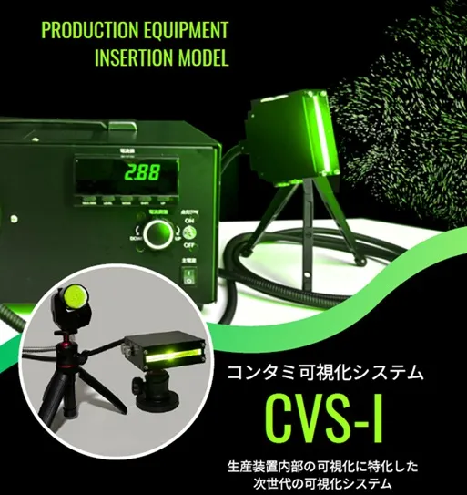
CVS(Contamination Vizualization System)
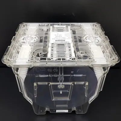
Wafer
Dummy Wafer is essential to maintain tool stability and yield in semiconductor manufacturing process.
We handle a widely range spec of wafers and supply steadily.
Consumables Quartz, Si, Resin, O-rings, etc.
These precision and consumable parts are key to maintain chamber best condition, we handle like this parts widely.